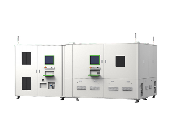
In the photovoltaic (PV) and semiconductor industries, boron doping is a critical step for adjusting material conductivity—it creates p-type semiconductors, laying the foundation for battery current generation. But traditional doping methods (like high-temperature thermal diffusion or plasma doping) often cause problems: excessive heat warps thin solar cells, while harsh chemical processes corrode cell surfaces, reducing yield by 8%–12%. This is where Boron Doping Equipment with a gentle doping process stands out: it uses controlled energy input and precise dopant delivery to achieve uniform boron distribution, cutting cell damage rates to less than 2% while maintaining doping efficiency. Let’s explore its real-world applications and answer common questions from manufacturers.
Core Application Industries & Scenarios
Photovoltaic (PV) Cell Manufacturing
High-efficiency PV cells—such as PERC, TOPCon, and HJT cells—rely on precise boron doping to optimize front-side emitters or back-side contacts. Gentle-process boron doping equipment is a game-changer here: it adapts to ultra-thin silicon wafers (thickness as low as 120μm) by regulating doping temperature (kept 30% lower than traditional methods) and using a low-pressure dopant source. For example, a PV manufacturer producing HJT cells previously struggled with 5% wafer breakage during boron doping; after adopting the equipment, breakage dropped to 0.8%, and the cells’ fill factor (a key efficiency indicator) increased by 2.3%. The gentle process also preserved the cell’s anti-reflective coating, reducing post-doping rework by 50%.
Semiconductor Wafer Production
Semiconductor wafers for microelectronics (like IoT sensors or power chips) need localized boron doping with minimal damage. The equipment’s micro-focused doping technology meets this demand: it targets specific wafer areas (down to 100μm in diameter) without affecting adjacent regions. A semiconductor manufacturer reported that using the equipment for boron doping on 8-inch silicon wafers reduced surface defect density from 15 defects/cm² to 3 defects/cm². This is crucial for small-scale semiconductor devices, where even tiny damage can cause short circuits or performance failure.
New-Generation Thin-Film Battery R&D
Thin-film batteries (such as CIGS or perovskite PV cells) are more fragile than traditional silicon cells, making gentle doping essential. Boron doping equipment’s adjustable process parameters (dopant concentration, energy intensity) let R&D teams test diverse doping schemes. A university’s PV lab used it to research perovskite-boron hybrid cells: the gentle process avoided perovskite layer decomposition, and they achieved a 19.5% conversion efficiency—5% higher than with traditional doping. The equipment’s automated data logging also simplified experiment analysis, accelerating R&D by 2 months.
Frequently Asked Questions (FAQ)
Q: Can the equipment handle different boron doping concentrations for various cell types?
A: Absolutely! It supports boron doping concentrations from 10¹⁵ to 10²⁰ atoms/cm³—covering all mainstream PV and semiconductor cell needs. You just input the target concentration and cell material into the touchscreen; the equipment automatically adjusts dopant flow rate and energy input. Switching from a 10¹⁷ atoms/cm³ doping for PERC cells to 10¹⁹ atoms/cm³ for power semiconductors takes only 10 minutes, no manual hardware tweaks needed.
Q: How does the gentle process affect doping uniformity?
A: It boosts uniformity! Traditional high-temperature methods cause dopant segregation (uneven distribution), but this equipment uses a multi-nozzle dopant delivery system and real-time temperature monitoring to ensure ±3% uniformity across the cell surface. A PV manufacturer verified that after doping, their cell’s sheet resistance variation dropped from ±8% to ±2%, directly improving batch-to-batch performance consistency.
Q: Is it easy to integrate the equipment into existing production lines?
A: Yes! It has a modular design that fits standard 1.2m–1.5m production line widths and connects to ERP/MES systems via Ethernet for real-time data tracking. The automated loading/unloading module works with existing conveyors, and workers only need 1 day of training to master basic operations. Most manufacturers can complete integration and start production within 1 week.
A high-tech enterprise specializing in automated precision laser and semiconductor equipment ensures its boron doping solutions meet strict quality standards, with nationwide after-sales support to resolve technical issues quickly—further safeguarding production efficiency for clients.


 Phone
Phone
Comment
(0)